Schmitt trigger

In electronics, a Schmitt trigger is a comparator circuit with hysteresis implemented by applying positive feedback to the noninverting input of a comparator or differential amplifier. It is an active circuit which converts an analog input signal to a digital output signal. The circuit is named a "trigger" because the output retains its value until the input changes sufficiently to trigger a change. In the non-inverting configuration, when the input is higher than a chosen threshold, the output is high. When the input is below a different (lower) chosen threshold the output is low, and when the input is between the two levels the output retains its value. This dual threshold action is called hysteresis and implies that the Schmitt trigger possesses memory and can act as a bistable multivibrator (latch or flip-flop). There is a close relation between the two kinds of circuits: a Schmitt trigger can be converted into a latch and a latch can be converted into a Schmitt trigger.
Schmitt trigger devices are typically used in signal conditioning applications to remove noise from signals used in digital circuits, particularly mechanical contact bounce in switches. They are also used in closed loop negative feedback configurations to implement relaxation oscillators, used in function generators and switching power supplies.

Contents
Invention[edit]
The Schmitt trigger was invented by American scientist Otto H. Schmitt in 1934 while he was a graduate student,[1] later described in his doctoral dissertation (1937) as a "thermionic trigger."[2] It was a direct result of Schmitt's study of the neural impulse propagation in squid nerves.[2]
Implementation[edit]
Fundamental idea[edit]

A > 1 is the amplifier gain
B < 1 is the feedback transfer function
Circuits with hysteresis are based on the fundamental positive feedback idea: any active circuit can be made to behave as a Schmitt trigger by applying a positive feedback so that the loop gain is more than one. The positive feedback is introduced by adding a part of the output voltage to the input voltage. These circuits contain an 'attenuator' (the B box in the figure on the right) and a 'summer' (the circle with "+" inside) in addition to an amplifier acting as a comparator. There are three specific techniques for implementing this general idea. The first two of them are dual versions (series and parallel) of the general positive feedback system. In these configurations, the output voltage increases the effective difference input voltage of the comparator by 'decreasing the threshold' or by 'increasing the circuit input voltage'; the threshold and memory properties are incorporated in one element. In the third technique, the threshold and memory properties are separated.
Dynamic threshold (series feedback): when the input voltage crosses the threshold in some direction the circuit itself changes its own threshold to the opposite direction. For this purpose, it subtracts a part of its output voltage from the threshold (it is equal to adding voltage to the input voltage). Thus the output affects the threshold and does not impact on the input voltage. These circuits are implemented by a differential amplifier with 'series positive feedback' where the input is connected to the inverting input and the output - to the non-inverting input. In this arrangement, attenuation and summation are separated: a voltage divider acts as an attenuator and the loop acts as a simple series voltage summer. Examples are the classic transistor emitter-coupled Schmitt trigger, the op-amp inverting Schmitt trigger, etc.
Modified input voltage (parallel feedback): when the input voltage crosses the threshold in some direction the circuit changes its input voltage in the same direction (now it adds a part of its output voltage directly to the input voltage). Thus the output augments the input voltage and does not affect the threshold. These circuits can be implemented by a single-ended non-inverting amplifier with 'parallel positive feedback' where the input and the output sources are connected through resistors to the input. The two resistors form a weighted parallel summer incorporating both the attenuation and summation. Examples are the less familiar collector-base coupled Schmitt trigger, the op-amp non-inverting Schmitt trigger, etc.
Some circuits and elements exhibiting negative resistance can also act in a similar way: negative impedance converters (NIC), neon lamps, tunnel diodes (e.g., a diode with an "N"-shaped current–voltage characteristic in the first quadrant), etc. In the last case, an oscillating input will cause the diode to move from one rising leg of the "N" to the other and back again as the input crosses the rising and falling switching thresholds.
Two different unidirectional thresholds are assigned in this case to two separate open-loop comparators (without hysteresis) driving a bistable multivibrator (latch) or flip-flop. The trigger is toggled high when the input voltage crosses down to up the high threshold and low when the input voltage crosses up to down the low threshold. Again, there is a positive feedback but now it is concentrated only in the memory cell. Examples are the 555 timer and the switch debounce circuit.[3]

The symbol for Schmitt triggers in circuit diagrams is a triangle with a symbol inside representing its ideal hysteresis curve.
Transistor Schmitt triggers[edit]
Classic emitter-coupled circuit[edit]
The original Schmitt trigger is based on the dynamic threshold idea that is implemented by a voltage divider with a switchable upper leg (the collector resistors RC1 and RC2) and a steady lower leg (RE). Q1 acts as a comparator with a differential input (Q1 base-emitter junction) consisting of an inverting (Q1 base) and a non-inverting (Q1 emitter) inputs. The input voltage is applied to the inverting input; the output voltage of the voltage divider is applied to the non-inverting input thus determining its threshold. The comparator output drives the second common collector stage Q2 (an emitter follower) through the voltage divider R1-R2. The emitter-coupled transistors Q1 and Q2 actually compose an electronic double throw switch that switches over the upper legs of the voltage divider and changes the threshold in a different (to the input voltage) direction.
This configuration can be considered as a differential amplifier with series positive feedback between its non-inverting input (Q2 base) and output (Q1 collector) that forces the transition process. There is also a smaller negative feedback introduced by the emitter resistor RE. To make the positive feedback dominate over the negative one and to obtain a hysteresis, the proportion between the two collector resistors is chosen RC1 > RC2. Thus less current flows through and less voltage drop is across RE when Q1 is switched on than in the case when Q2 is switched on. As a result, the circuit has two different thresholds in regard to ground (V− in the image).
Operation[edit]
Initial state. For the NPN transistors shown on the right, imagine the input voltage is below the shared emitter voltage (high threshold for concreteness) so that Q1 base-emitter junction is reverse-biased and Q1 does not conduct. The Q2 base voltage is determined by the mentioned divider so that Q2 is conducting and the trigger output is in the low state. The two resistors RC2 and RE form another voltage divider that determines the high threshold. Neglecting VBE, the high threshold value is approximately
- .

The output voltage is low but well above ground. It is approximately equal to the high threshold and may not be low enough to be a logical zero for next digital circuits. This may require additional shifting circuit following the trigger circuit.
Crossing up the high threshold. When the input voltage (Q1 base voltage) rises slightly above the voltage across the emitter resistor RE (the high threshold), Q1 begins conducting. Its collector voltage goes down and Q2 begins going cut-off, because the voltage divider now provides lower Q2 base voltage. The common emitter voltage follows this change and goes down thus making Q1 conduct more. The current begins steering from the right leg of the circuit to the left one. Although Q1 is more conducting, it passes less current through RE (since RC1 > RC2); the emitter voltage continues dropping and the effective Q1 base-emitter voltage continuously increases. This avalanche-like process continues until Q1 becomes completely turned on (saturated) and Q2 turned off. The trigger is transitioned to the high state and the output (Q2 collector) voltage is close to V+. Now, the two resistors RC1 and RE form a voltage divider that determines the low threshold. Its value is approximately
- .

Crossing down the low threshold. With the trigger now in the high state, if the input voltage lowers enough (below the low threshold), Q1 begins cutting-off. Its collector current reduces; as a result, the shared emitter voltage lowers slightly and Q1 collector voltage rises significantly. The R1-R2 voltage divider conveys this change to the Q2 base voltage and it begins conducting. The voltage across RE rises, further reducing the Q1 base-emitter potential in the same avalanche-like manner, and Q1 ceases to conduct. Q2 becomes completely turned on (saturated) and the output voltage becomes low again.
Variations[edit]

Non-inverting circuit. The classic non-inverting Schmitt trigger can be turned into an inverting trigger by taking Vout from the emitters instead of from a Q2 collector. In this configuration, the output voltage is equal to the dynamic threshold (the shared emitter voltage) and both the output levels stay away from the supply rails. Another disadvantage is that the load changes the thresholds so, it has to be high enough. The base resistor RB is obligatory to prevent the impact of the input voltage through Q1 base-emitter junction on the emitter voltage.
Direct-coupled circuit. To simplify the circuit, the R1–R2 voltage divider can be omitted connecting Q1 collector directly to Q2 base. The base resistor RB can be omitted as well so that the input voltage source drives directly Q1's base.[4] In this case, the common emitter voltage and Q1 collector voltage are not suitable for outputs. Only Q2 collector should be used as an output since, when the input voltage exceeds the high threshold and Q1 saturates, its base-emitter junction is forward biased and transfers the input voltage variations directly to the emitters. As a result, the common emitter voltage and Q1 collector voltage follow the input voltage. This situation is typical for over-driven transistor differential amplifiers and ECL gates.
Collector-base coupled circuit[edit]

Like every latch, the fundamental collector-base coupled bistable circuit possesses a hysteresis. So, it can be converted to a Schmitt trigger by connecting an additional base resistor R to one of the inputs (Q1 base in the figure). The two resistors R and R4 form a parallel voltage summer (the circle in the ballock diagram above) that sums output (Q2 collector) voltage and the input voltage, and drives the single-ended transistor "comparator" Q1. When the base voltage crosses the threshold (VBE0 ∞ 0.65 V) in some direction, a part of Q2's collector voltage is added in the same direction to the input voltage. Thus the output modifies the input voltage by means of parallel positive feedback and does not affect the threshold (the base-emitter voltage).
Comparison between emitter- and collector-coupled circuit[edit]
The emitter-coupled version has the advantage that the input transistor is reverse biased when the input voltage is quite below the high threshold so the transistor is surely cut-off. It was important when germanium transistors were used for implementing the circuit and this advantage has determined its popularity. The input base resistor can be omitted since the emitter resistor limits the current when the input base-emitter junction is forward-biased.
An emitter-coupled Schmitt trigger logical zero output level may not be low enough and might need an additional output shifting circuit. The collector-coupled Schmitt trigger has extremely low (almost zero) output at logical zero.
Op-amp implementations[edit]
Schmitt triggers are commonly implemented using an operational amplifier or a dedicated comparator.[nb 2] An open-loop op-amp and comparator may be considered as an analog-digital device having analog inputs and a digital output that extracts the sign of the voltage difference between its two inputs.[nb 3] The positive feedback is applied by adding a part of the output voltage to the input voltage in series or parallel manner. Due to the extremely high op-amp gain, the loop gain is also high enough and provides the avalanche-like process.
Non-inverting Schmitt trigger[edit]

In this circuit, the two resistors R1 and R2 form a parallel voltage summer. It adds a part of the output voltage to the input voltage thus augmenting it during and after switching that occurs when the resulting voltage is near ground. This parallel positive feedback creates the needed hysteresis that is controlled by the proportion between the resistances of R1 and R2. The output of the parallel voltage summer is single-ended (it produces voltage with respect to ground) so the circuit does not need an amplifier with a differential input. Since conventional op-amps have a differential input, the inverting input is grounded to make the reference point zero volts.
The output voltage always has the same sign as the op-amp input voltage but it does not always have the same sign as the circuit input voltage (the signs of the two input voltages can differ). When the circuit input voltage is above the high threshold or below the low threshold, the output voltage has the same sign as the circuit input voltage (the circuit is non-inverting). It acts like a comparator that switches at a different point depending on whether the output of the comparator is high or low. When the circuit input voltage is between the thresholds, the output voltage is undefined and it depends on the last state (the circuit behaves as an elementary latch).
For instance, if the Schmitt trigger is currently in the high state, the output will be at the positive power supply rail (+VS). The output voltage V+ of the resistive summer can be found by applying the superposition theorem:

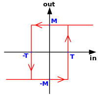
The comparator will switch when V+=0. Then (the same result can be obtained by applying the current conservation principle). So must drop below to get the output to switch. Once the comparator output has switched to −VS, the threshold becomes to switch back to high. So this circuit creates a switching band centered on zero, with trigger levels (it can be shifted to the left or the right by applying a bias voltage to the inverting input). The input voltage must rise above the top of the band, and then below the bottom of the band, for the output to switch on (plus) and then back off (minus). If R1 is zero or R2 is infinity (i.e., an open circuit), the band collapses to zero width, and it behaves as a standard comparator. The transfer characteristic is shown in the picture on the left. The value of the threshold T is given by and the maximum value of the output M is the power supply rail.


A unique property of circuits with parallel positive feedback is the impact on the input source.[citation needed] In circuits with negative parallel feedback (e.g., an inverting amplifier), the virtual ground at the inverting input separates the input source from the op-amp output. Here there is no virtual ground, and the steady op-amp output voltage is applied through R1-R2 network to the input source. The op-amp output passes an opposite current through the input source (it injects current into the source when the input voltage is positive and it draws current from the source when it is negative).
A practical Schmitt trigger with precise thresholds is shown in the figure on the right. The transfer characteristic has exactly the same shape of the previous basic configuration, and the threshold values are the same as well. On the other hand, in the previous case, the output voltage was depending on the power supply, while now it is defined by the Zener diodes (which could also be replaced with a single double-anode Zener diode). In this configuration, the output levels can be modified by appropriate choice of Zener diode, and these levels are resistant to power supply fluctuations (i.e., they increase the PSRR of the comparator). The resistor R3 is there to limit the current through the diodes, and the resistor R4 minimizes the input voltage offset caused by the comparator's input leakage currents (see limitations of real op-amps).
Inverting Schmitt trigger[edit]

In the inverting version, the attenuation and summation are separated. The two resistors R1 and R2 act only as a "pure" attenuator (voltage divider). The input loop acts as a simple series voltage summer that adds a part of the output voltage in series to the circuit input voltage. This series positive feedback creates the needed hysteresis that is controlled by the proportion between the resistances of R1 and the whole resistance (R1 and R2). The effective voltage applied to the op-amp input is floating so the op-amp must have a differential input.
The circuit is named inverting since the output voltage always has an opposite sign to the input voltage when it is out of the hysteresis cycle (when the input voltage is above the high threshold or below the low threshold). However, if the input voltage is within the hysteresis cycle (between the high and low thresholds), the circuit can be inverting as well as non-inverting. The output voltage is undefined and it depends on the last state so the circuit behaves like an elementary latch.
To compare the two versions, the circuit operation will be considered at the same conditions as above. If the Schmitt trigger is currently in the high state, the output will be at the positive power supply rail (+VS). The output voltage V+ of the voltage divider is:

The comparator will switch when Vin = V+. So must exceed above this voltage to get the output to switch. Once the comparator output has switched to −VS, the threshold becomes to switch back to high. So this circuit creates a switching band centered on zero, with trigger levels (it can be shifted to the left or the right by connecting R1 to a bias voltage). The input voltage must rise above the top of the band, and then below the bottom of the band, for the output to switch off (minus) and then back on (plus). If R1 is zero (i.e., a short circuit) or R2 is infinity, the band collapses to zero width, and it behaves as a standard comparator.


In contrast with the parallel version, this circuit does not impact on the input source since the source is separated from the voltage divider output by the high op-amp input differential impedance.
In the inverting amplifier voltage drop across resistor (R1) decides the reference voltages i.e.,upper threshold voltage (V+) and lower threshold voltages (V-) for the comparison with input signal applied. These voltages are fixed as the output voltage and resistor values are fixed.
so by changing the drop across (R1) threshold voltages can be varied. By adding a bias voltage in series with resistor (R1) drop across it can be varied, which can change threshold voltages. Desired values of reference voltages can be obtained by varying bias voltage.
The above equations can be modified as

Applications[edit]
Schmitt triggers are typically used in open loop configurations for noise immunity and closed loop configurations to implement function generators.
- Analog to digital conversion: The Schmitt trigger is effectively a one bit analog to digital converter. When the signal reaches a given level it switches from its low to high state.
- Level detection: The Schmitt trigger circuit is able to provide level detection. When undertaking this application, it is necessary that the hysteresis voltage is taken into account so that the circuit switches on the required voltage.
- Line reception: When running a data line that may have picked up noise into a logic gate it is necessary to ensure that a logic output level is only changed as the data changed and not as a result of spurious noise that may have been picked up. Using a Schmitt trigger broadly enables the peak to peak noise to reach the level of the hysteresis before spurious triggering may occur.
Noise immunity[edit]
One application of a Schmitt trigger is to increase the noise immunity in a circuit with only a single input threshold. With only one input threshold, a noisy input signal [nb 4] near that threshold could cause the output to switch rapidly back and forth from noise alone. A noisy Schmitt Trigger input signal near one threshold can cause only one switch in output value, after which it would have to move beyond the other threshold in order to cause another switch.
For example, an amplified infrared photodiode may generate an electric signal that switches frequently between its absolute lowest value and its absolute highest value. This signal is then low-pass filtered to form a smooth signal that rises and falls corresponding to the relative amount of time the switching signal is on and off. That filtered output passes to the input of a Schmitt trigger. The net effect is that the output of the Schmitt trigger only passes from low to high after a received infrared signal excites the photodiode for longer than some known period, and once the Schmitt trigger is high, it only moves low after the infrared signal ceases to excite the photodiode for longer than a similar known period. Whereas the photodiode is prone to spurious switching due to noise from the environment, the delay added by the filter and Schmitt trigger ensures that the output only switches when there is certainly an input stimulating the device.
Schmitt triggers are common in many switching circuits for similar reasons (e.g., for switch debouncing).

The following 7400 series devices include a Schmitt trigger on their input or on each of their inputs:
- 7413: Dual Schmitt trigger 4-input NAND Gate
- 7414: Hex Schmitt trigger Inverter
- 7418: Dual Schmitt trigger 4-input NAND Gate
- 7419: Hex Schmitt trigger Inverter
- 74121: Monostable Multivibrator with Schmitt Trigger Inputs
- 74132: Quad 2-input NAND Schmitt Trigger
- 74221: Dual Monostable Multivibrator with Schmitt Trigger Input
- 74232: Quad NOR Schmitt Trigger
- 74310: Octal Buffer with Schmitt Trigger Inputs
- 74340: Octal Buffer with Schmitt Trigger Inputs and three-state inverted outputs
- 74341: Octal Buffer with Schmitt Trigger Inputs and three-state noninverted outputs
- 74344: Octal Buffer with Schmitt Trigger Inputs and three-state noninverted outputs
- 74(HC/HCT)7541 Octal Buffer with Schmitt Trigger Inputs and Three-State Noninverted Outputs
- SN74LV8151 is a 10-bit universal Schmitt-trigger buffer with 3-state outputs
A number of 4000 series devices include a Schmitt trigger on inputs, for example:
- 4017: Decade Counter with Decoded Outputs
- 4020: 14-Stage Binary Ripple Counter
- 4022: Octal Counter with Decoded Outputs
- 4024: 7-Stage Binary Ripple Counter
- 4040: 12-Stage Binary Ripple Counter
- 4093: Quad 2-Input NAND
- 40106: Hex Inverter
- 14538: Dual Monostable Multivibrator
Dual Schmitt input configurable single-gate CMOS logic, AND, OR, XOR, NAND, NOR, XNOR
- NC7SZ57 Fairchild
- NC7SZ58 Fairchild
- SN74LVC1G57 Texas Instruments
- SN74LVC1G58 Texas Instruments
Use as an oscillator[edit]


A Schmitt trigger is a bistable multivibrator, and it can be used to implement another type of multivibrator, the relaxation oscillator. This is achieved by connecting a single RC integrating circuit between the output and the input of an inverting Schmitt trigger. The output will be a continuous square wave whose frequency depends on the values of R and C, and the threshold points of the Schmitt trigger. Since multiple Schmitt trigger circuits can be provided by a single integrated circuit (e.g. the 4000 series CMOS device type 40106 contains 6 of them), a spare section of the IC can be quickly pressed into service as a simple and reliable oscillator with only two external components.
Here, a comparator-based Schmitt trigger is used in its inverting configuration. Additionally, slow negative feedback is added with an integrating RC network. The result, which is shown on the right, is that the output automatically oscillates from VSS to VDD as the capacitor charges from one Schmitt trigger threshold to the other.
See also[edit]
- Operational amplifier applications
- Bistable multivibrator circuit
- Threshold detector with hysteresis
Notes[edit]
- ^ One factor contributing to ambiguity is that one simple transistor-based realization of a Schmitt trigger is naturally inverting, with a non-inverting Schmitt trigger sometimes consisting of such an inverting implementation followed by an inverter. An additional inverter may be added for buffering a stand-alone inverting configuration. Consequently, inverting configurations within an integrated circuit may be naturally inverting, while non-inverting configurations are implemented with a single inverter, and stand-alone inverting configurations may be implemented with two inverters. As a result, symbols that combine inverting bubbles and hysteresis curves may be using the hysteresis curve to describe the entire device or the embedded Schmitt trigger only.
- ^ Usually, negative feedback is used in op-amp circuits. Some operational amplifiers are designed to be used only in negative-feedback configurations that enforce a negligible difference between the inverting and non-inverting inputs. They incorporate input-protection circuitry that prevent the inverting and non-inverting inputs from operating far away from each other. For example, clipper circuits made up of two general purpose diodes with opposite bias in parallel [1] or two Zener diodes with opposite bias in series (i.e., a double-anode Zener diode) are sometimes used internally across the two inputs of the operational amplifier. In these cases, the operational amplifiers will fail to function well as comparators. Conversely, comparators are designed under the assumption that the input voltages can differ significantly.
- ^ When the non-inverting (+) input is at a higher voltage than the inverting (−) input, the comparator output switches nearly to +VS, which is its high supply voltage. When the non-inverting (+) input is at a lower voltage than the inverting (−) input, the comparator output switches nearly to -VS, which is its low supply voltage.
- ^ Where the noise amplitude is assumed to be small compared to the change in Schmitt trigger threshold.
References[edit]
- ^ Otto H. Schmitt, A Thermionic Trigger, Journal of Scientific Instruments 15 (January 1938): 24–26.
- ^ a b August 2004 issue of the Pavek Museum of Broadcasting Newsletter - http://160.94.102.47/Otto_Images/PavekOHSbio.pdf
- ^ Debouncing switches with an SR latch
- ^ 7414 datasheet
External links[edit]
| Wikimedia Commons has media related to Schmitt triggers. |